


Besides analog channels, state-of-the-art mixed signal oscilloscopes also include digital channels to analyze digital states and protocol details. Developers of embedded designs need to perform a diverse range of measurements during the initial operation of a new module. Analog signals from components such as A/D converters and power supplies need to be analyzed along with digital signals on serial and parallel data buses. As development cycles continue to grow shorter, the pressure is increasing to finish such analysis work as fast as possible. This is why comprehensive integrated measurement tools that can deliver reliable measurement results are critical for today's developers.
Evaluation of Analog Signals
To efficiently analyze a module with an A/D converter using an advanced mixed signal oscilloscope (MSO), it is important to evaluate the analog signal characteristics as well as the quality of the A/D converter input signal. In terms of its digital circuitry, the A/D converter output must function correctly and the SPI control commands must be correctly interpreted. Naturally, the clock signal plays an important role in the proper operation of the A/D converter. Finally, the quality of the power supply must be tested.
High Acquisition Rate
As an initial step in the debugging process, the main signal of interest – the A/D converter input signal in this case – is viewed with the oscilloscope to see if any rare faults such as glitches or runts are present in the signal. Advanced digital oscilloscopes such as the R&S RTE provide a high acquisition rate of up to 1 million waveforms/s, allowing defects to be eliminated relatively quickly with a high degree of probability.
The oscilloscope R&S RTE QuickMeas function allows users to obtain a fast overview of the signal characteristics. For the chosen signal, QuickMeas simultaneously displays the results of multiple user-defined measurement functions, for example the frequency, peak-to-peak voltage and RMS value for the A/D converter input signal.
If the user wants measurement results not currently included by QuickMeas, additional automatic measurement functions can be activated, including statistical evaluation. A high acquisition and processing rate is necessary to enable a statistically meaningful analysis, thereby ensuring that even complex measurement series can be handled quickly. In addition to the fundamental and harmonics, other influences and interference factors such as sporadic or intermittent signals can be detected and analyzed in the signal's spectrum.
For detection and precise measurement of weak signals, the oscilloscope must have a low-noise analog frontend with a wide dynamic range and high input sensitivity without bandwidth limitations. The FFT function provided by the R&S RTE also makes the user's job much easier: operation is as simple as entering the center frequency, span and resolution bandwidth.
Analysis of Parallel Data Buses
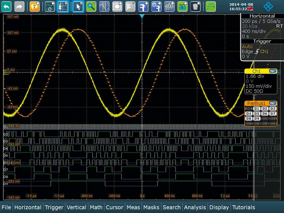
Integrated logic analysis makes it possible to display time-correlated digital signals with analog waveforms. The R&S RTE mixed signal option turns the oscilloscope into an easy-to-use MSO with 16 digital channels. In this example, the output of the A/D converter has nine lines (corresponding to eight data bits and a clock signal). The logic state of the bus is determined for valid edges of the clock signal. The user configures the parallel bus according to the actual bus topology and defines which digital channels are part of the bus and where the binarization decision threshold is placed.
The R&S RTE oscilloscopes support simultaneous decoding of four parallel or serial buses. Each bus is represented by an icon on the edge of the screen. Regardless of the other oscilloscope settings, the icon shows the current status of all activated logic channels (high, low, toggle) to give the user a fast overview of bus activity. This also includes the channels that are not displayed in the diagram. Of course, the decoded bus can be presented in a bus format. This allows direct comparison of the input and output signals as well as measurement of the time offset between the two signals, for example. Any distortion present in the output signal is also clearly visible.
High Sampling Rate
The frequent spikes in the analog bus display are a clear indication of problems in module design. These narrow spikes are visible thanks to the high sampling rate of 5 GSample/s per digital channel, which is equivalent to a time resolution of
200 ps.
In the R&S RTE, this sampling rate is available across the entire
100 MSample memory depth so that even spikes that occur long after the trigger point can be detected. It is logical to assume such spikes are caused by timing problems leading to a violation of the setup and hold time.
The setup time determines how long a data signal must be present prior to the next clock edge. The hold time indicates how long the data signal must remain constant after a clock edge to be valid. In order to test whether our assumption is correct, all we have to do is offset the timing of the clock signal in the oscilloscope relative to the data signals.
Advanced oscilloscopes such as the R&S RTE are capable of individually offsetting any digital channel with respect to all other channels. An offset of only 2 ns for example is sufficient to eliminate the spikes from the analog bus representation. Based on this insight, the user can review the design and make any necessary changes in the signal path lengths.
Testing Serial Communications
The A/D converter output is controlled by an SPI interface. Here, the developer must verify that the transmission process is working properly and that the timing interplay between the programming interface and the operation of the module is in line with the specification. In addition to user data, serial bus signals include control and address information that is embedded in a frame. Consequently, additional software support is typically required for debugging systems that use serial data buses.
Isolating protocol-specific events becomes easier if the oscilloscope can trigger on the content of the serial protocol that is being used and display the decoded message. Accordingly, the oscilloscope must support triggering and decoding of protocols for widely used serial interfaces such as I2C, UART/RS-232, CAN and SPI. While testing SPI communications, the user can minimize the display of the analog A/D converter input signal and the parallel data bus at the output to make the whole screen available. However, a clear overview is maintained since miniature views of the minimized signals remain visible in realtime on the edge of the screen.
Another important element in the debugging process is determining the response time between when an SPI command ends and when the A/D converter output signal starts. The cursor function allows easy measurement of the time difference. On the R&S RTE, the user can just drag and drop the A/D converter output signal icon back to the screen. The SPI sequence and the parallel bus can be displayed in a single diagram or in two separate diagrams.
Next, the oscilloscope's timebase should be reduced until a meaningful measurement can be performed. The cursor function makes it easy to measure the time that is required by the A/D converter in this example to respond to the SPI activation command. The user can flexibly position the result window on the screen.
Conclusion
Mixed signal oscilloscopes are one of the most important test instruments for developing and debugging new electronic circuits. They are a valuable tool for hardware developers when analyzing signal integrity and for software developers when analyzing the content of signals. The R&S RTE oscilloscopes from Rohde & Schwarz support time domain, logic, protocol and frequency analysis. In addition, the very precise DC voltmeter (measurement error ±0.1 percent) integrated in the tip of the active probes provides a convenient way to answer questions such as "Is the supply voltage correct?" and "Is a DC voltage superimposed?" As a result, the different components of embedded designs – along with their interactions – can be analyzed with just a single test instrument. The benefits for users include simpler test setups, a single user interface and synchronized visualization of analog waveforms, digital signals and protocol details.