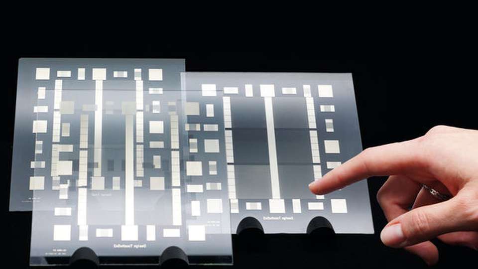
The Future of Touchscreens
To make the touchscreens work, they are provided on their surface with microscopically small electrical conductor tracks, which detect the position when touched with a finger. At the peripheries of the devices, these microscopic tracks merge into larger conductor tracks. Until now, several production stages have been needed to create them. The researchers at the INM – Leibniz-Institute for New Materials are now presenting a novel process that allows microscopic and macroscopic conductor tracks to be produced in one step. The developers are basing the novel process on photometallization: under exposure to UV light, and acting in conjunction with a photoactive layer, colourless silver compounds turn into electrically conductive silver. The silver compound can be applied in the form of tracks or other structures to plastic films or glass by various methods. Tracks of various sizes, down to the smallest size of a 1000th of a millimetre, can be created in this way. The corresponding conductor tracks are then produced by exposure to UV light. The foils or glass are first coated with a photoactive layer of metal oxide nanoparticles. “We then apply the colourless, UV-stable silver compound”, says Peter William de Oliveira, Head of the Optical Materials Program Division. The exposure of this series of layers has the effect that the silver compound on the photoactive layer decomposes and the silver ions are reduced to metallic, electrically conductive silver. This process is said to have several advantages: it is claimed to be quick, flexible, variable in scale, low in cost and environmentally friendly. And there is no need for any further post-treatment process steps.


